
 poe@pcbamake.com


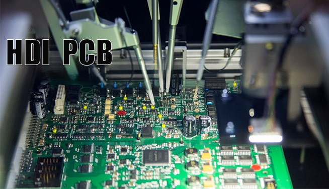
HDI PCB is a circuit board design technology with high density and high performance, and it is a compact circuit board designed for small capacity users. It has been improved and innovated on the basis of traditional PCB. Compared with traditional PCBs, HDI PCBs have significant advantages in many aspects. HDI pcb is a special pcb board in pcb board.
Main features of HDI PCB
HDI PCB has high density, high performance and high reliability.
HDI PCB can achieve higher circuit density, making electronic equipment more powerful and higher performance while maintaining a smaller size.
HDI PCB also has good maintainability and anti-interference ability, suitable for complex electronic systems and high-speed data transmission application scenarios.
HDI PCB application scenarios
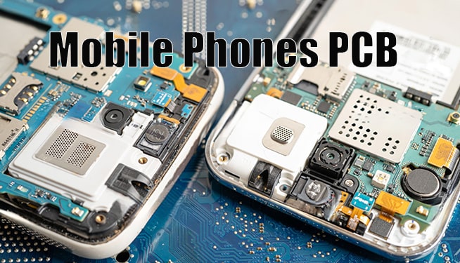
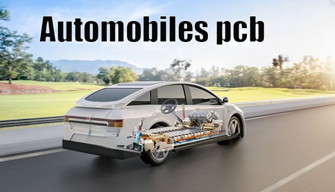
HDI pcb is mainly used in mobile phones, automobiles, medical equipment, touch screen equipment, notebook computers, digital cameras, and 4G network communications.
Mobile phones: HDI PCB circuit boards can improve the signal quality, battery life and functional integration of mobile phones, while reducing the weight and thickness of mobile phones. HDI PCB circuit boards can also support the development of new technologies such as 5G communications, artificial intelligence and the Internet of Things.
Automobiles: HDI PCB circuit boards can meet the complexity and reliability requirements of automotive electronic systems, while improving the safety, comfort and intelligence of
automobiles. HDI PCB circuit boards can also be used in functions such as automotive radar, navigation, entertainment and driving assistance.
Medical: HDI PCB circuit board can improve the precision, sensitivity and stability of medical equipment, while reducing the volume and power consumption of medical equipment. HDI PCB circuit boards can also be used in medical imaging, monitoring, diagnosis and treatment.

What are the advantages of HDI PCB over ordinary PCB
line density
The most common reason for using HDI technology in PCBA production is to significantly increase packaging density. By using higher-level packaging technology and smaller aperture, HDI PCB can achieve higher circuit density within the same size. The space gained by the finer track structure can be used for components. Additionally, the reduction in overall space requirements will result in smaller board sizes and fewer layers.
In SMT processing, usually FPGA or BGA can provide a pitch of 1mm or less. HDI technology makes wiring and connections easy, especially when routing between pins.
Signal Integrity and Electromagnetic Compatibility
HDI PCB uses more advanced materials and manufacturing processes, which can provide better signal integrity and electromagnetic compatibility. This is beneficial for high-speed data transmission and high-frequency applications, as they have high requirements on signal quality and immunity to interference. In contrast, traditional PCBs may not be able to achieve the same level in these aspects.
Maintainability and Reliability
The design of HDI PCB is more complex and refined, which can achieve a higher degree of automation. This makes HDI PCB easier to carry out on-line detection and fault diagnosis during the production process, thus improving the maintainability and reliability of the product. In addition, HDI PCBs can also use more durable materials and packaging techniques to further extend the life of the device.
Cost-effectiveness
The manufacturing cost of HDI PCB is usually higher than ordinary ones, but due to its high circuit density, high performance and high reliability, as well as better maintainability and anti-interference ability, it can bring higher efficiency in long-term operation cost-effective. Especially for large electronic equipment or high-speed data transmission applications, choosing HDI PCB can bring greater value to users.
With the development of technology and the growing demand for high-performance electronic equipment, HDI PCB is expected to continue to play an important role in the future.
If you have PCB/PCBA/OEM/ODM needs, please contact us, We will reply within 2 hours, and complete the quotation within 4 hours or less upon request.
Delivery Services

Verified by

Link Us on


