Deep understanding of PCB back drilling
revealing the delicate craftsmanship behind the circuit board
In the world of electronic manufacturing, PCB is an important part of the heart of electronic devices. It carries electronic components and connects them through conductive tracks to ensure smooth flow of current. But did you know? In the manufacturing process of PCB, there is a technology called "back drilling", which is essential for achieving high-speed, high-performance electronic devices.

What is PCB back drilling?
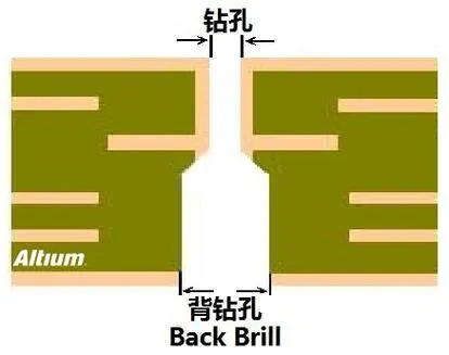
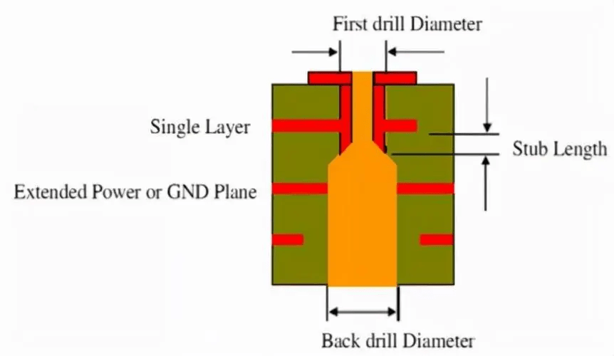
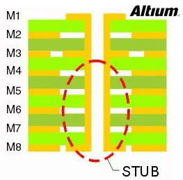
In simple terms, PCB back drilling is to drill holes from the back of the already made multi-layer circuit board, but this time it is not a random drilling, but to accurately remove some unnecessary parts of the through holes (PTH, Plated-Through Holes). These parts, we call them "stubs", they are like extra "tails" on the circuit board, although small, but can cause big problems in high-speed signal transmission.

The origin of back drilling
In multi-layer PCBs, through holes are bridges used to connect conductive tracks between different layers. They penetrate from one side of the board to the other side, allowing current and signals to flow smoothly between layers. However, sometimes these through holes are drilled deeper than they actually need to be, leaving a useless stub. These stubs are like antennas when transmitting high-speed signals, absorbing and reflecting signals, causing signal distortion and increased interference, thus affecting the performance of the entire circuit.

To solve this problem, engineers invented back drilling technology. It is like a precise "scissor hand" that is specifically responsible for cutting off these extra "tails" to make signal transmission smoother and unimpeded.
Back drilling technology sounds simple, but it is a technical job in actual operation. There are several key points that need special attention:
The "behind-the-scenes hero" of back drilling
In the PCB manufacturing process, back drilling technology is often the "hero" working silently behind the scenes. It is not as eye-catching as those conspicuous components and chips, but it plays an irreplaceable role in ensuring circuit performance and improving product quality. However, back drilling technology is not omnipotent. It is affected by many factors, such as the hardness and thickness of the PCB material, the accuracy of the drilling equipment, etc. Therefore, when performing back drilling, it is necessary to comprehensively consider various factors and select appropriate process parameters and equipment.
"Daily Application" of Back Drilling
Back drilling technology is also widely used in our daily life. For example, the electronic devices you are using, such as smartphones, tablets, and laptops, may use back drilling technology to optimize the performance of circuit boards. The reason why these devices can achieve high-speed and stable data and signal transmission is inseparable from the support of back drilling technology.
If you have PCB/PCBA/OEM/ODM needs, please contact us, We will reply within 2 hours, and complete the quotation within 4 hours or less upon request.