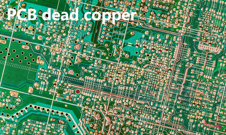
Possible problems caused by dead copper in PCB design
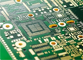
Dead copper (i.e. islanded copper) is a common problem during the PCB design process. Dead copper refers to areas of copper that are isolated on a circuit board without electrical connections. Many electronics engineers are often confused when they encounter dead copper and are unsure whether it needs to be removed.
Possible problems caused by dead copper
1. EMI issues
Dead copper may form an antenna effect on the circuit board, enhance the intensity of surrounding electromagnetic radiation, and easily accept external electromagnetic interference (EMI), thus affecting the normal operation of the circuit. Especially in high-frequency circuits, this effect is particularly significant and may cause serious degradation in circuit performance.

2. High frequency noise
In high frequency circuits, dead copper can become a medium for noise propagation. Isolated copper areas can pick up and propagate high-frequency noise, affecting the signal integrity and overall performance of the circuit, resulting in reduced circuit reliability.
Reasons to keep dead copper
1. Aesthetics
Cosmetically, removing dead copper leaves large empty areas on the board, which may not look aesthetically pleasing. For some design projects that have high requirements on appearance, retaining an appropriate amount of dead copper can enhance the overall visual effect.
2. Mechanical properties
The vectored dead copper area can increase the mechanical strength of the circuit board, help distribute stress evenly, and prevent the circuit board from bending or deforming under uneven stress. Especially in larger area circuit board designs, retaining dead copper can help enhance structural stability.
How to deal with dead copper?
1. Try to remove as much dead copper as possible
In order to reduce EMI and high-frequency PCB noise, it is recommended to remove dead copper as much as possible. Especially in high-frequency circuit designs, removing dead copper can avoid potential interference problems. If dead copper must be retained, it can be well connected to the ground layer (GND) through a ground hole (via) to form an effective shielding layer, thereby mitigating its impact on circuit performance.
2. Properly retain dead copper
In some cases, in order to consider the aesthetics and mechanical strength of the circuit board, some dead copper can be appropriately retained. It should be noted that these dead coppers must be connected to GND through ground holes to avoid forming an antenna effect. Also, make sure your traces are properly spaced to reduce negative impact on circuit performance.
3. Processing of high-frequency circuits
In high frequency circuits, dead copper must be handled with great caution. Even if it cannot be completely removed, make sure it is connected to GND through the ground hole to avoid the spread of high-frequency noise. At the same time, the wiring spacing should be as small as λ/20 of the noise frequency wavelength to reduce noise interference.
4. Comprehensive consideration
In actual design, whether to remove dead copper should be comprehensively considered based on the specific needs of the circuit and the working environment. For complex circuits and high-frequency circuits, it is recommended to conduct simulation analysis and actual testing to determine the best processing solution. Through a thorough evaluation, the best solution can be found that meets both electrical performance, mechanical and aesthetic needs.
In PCB design, whether it is necessary to remove dead copper needs to be analyzed on a case-by-case basis. For high-frequency and high-sensitivity circuits, removing dead copper as much as possible is the key to ensuring circuit performance. In other cases, proper retention of dead copper can improve the aesthetics and mechanical strength of the circuit board. Through reasonable design and processing, circuit performance and other needs can be effectively balanced to ensure the reliability and aesthetics of the final product.
If you want to know more, you can follow PCBAMake. If you need to know more technical knowledge about PCB proofing, SMT patching, and PCBA processing, please leave a message to get it!

