- Home
- About us
- Products
- PCB Fabrication
- PCB Assembly&OEM
- Quality
- Blogs
- Contact
One-Stop Turnkey PCB Assembly Manufacturer
PCB Assembly&OEM
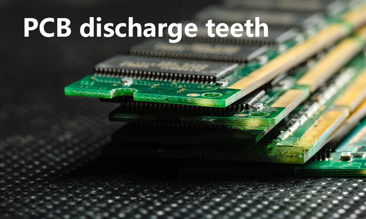
PCB discharge teeth refer to the discharge surface specially designed on the printed circuit board (PCB), usually a pair of triangles with sharp angles pointing to each other, made of copper foil layers used in the PCB design and wiring process. These triangles need to be placed on another layer of the PCB board components and cannot be covered by green oil or other coverings.

1. The role of PCB discharge teeth
Prevent static electricity accumulation: The discharge teeth can quickly conduct static electricity that contacts the circuit board, effectively preventing static electricity from accumulating and accumulating on the circuit board.
Protect electronic components: Static electricity damage to electronic components is often irreversible. The discharge teeth can absorb static electricity that contacts the circuit board and guide it to the ground or ground wire, thereby protecting the electronic components on the circuit board from static electricity damage and extending the life and reliability of electronic components.
Improve product quality: By adding discharge teeth and following relevant electrostatic protection measures, faults caused by static electricity can be reduced and the quality and reliability of products can be improved.
Comply with electronic industry standards: In some electronic industries, discharge teeth are required to meet the electrostatic protection standards of related electronic equipment and products.
In addition, during surge testing or ESD (electrostatic discharge) testing, high voltage may be generated at both ends of the common-mode inductor, causing arcing. If the distance to surrounding devices is close, surrounding devices may be damaged. Therefore, discharge teeth can be placed at both ends of the common-mode inductor to discharge through the tip of the discharge teeth, reduce or avoid discharge through other paths, and thus protect surrounding and downstream devices.
2. Design considerations
Position: The discharge teeth need to be set on another layer of PCB components to ensure that they are not covered by green oil and other coverings to ensure their discharge effect.
Shape and size: The discharge teeth are usually designed as a pair of acute triangles pointing to each other. The design of the tooth spacing needs to consider the air breakdown field strength and the requirements of the safety insulation withstand voltage test. For example, in dry air, when the ESD voltage is 3000V, the spacing of 1mm just reaches the critical field strength of breakdown discharge.
Material: The discharge teeth are made of copper foil layer, so they have good conductivity.
3. Application scenarios
PCB discharge teeth are widely used in electronic equipment and products that need to prevent electrostatic damage, such as communication equipment, computers and their peripherals, and household appliances. Especially in surge current voltage, ESD and other occasions, the discharge teeth can effectively protect circuit boards and electronic components from damage.
4. Disadvantages and maintenance
Carbon deposition problem: After the number of discharges increases, carbon deposition is easy to form between the discharge teeth, resulting in a decrease in the insulation resistance between the teeth. Especially in a humid environment, the carbon deposition problem may be more serious. Therefore, it is necessary to regularly clean the carbon deposition between the discharge teeth to maintain its good discharge effect.
Design limitations: The design of the discharge teeth needs to take into account the spacing and position relationship with components such as common mode inductors to avoid interference or damage to other components.
PCB discharge teeth are an important electrostatic protection component that can effectively prevent static electricity from damaging circuit boards and electronic components. However, during use, it is also necessary to pay attention to its design and maintenance issues to ensure its long-term and stable discharge effect.
If you have PCB/PCBA/OEM/ODM needs, please contact us, We will reply within 2 hours, and complete the quotation within 4 hours or less upon request.