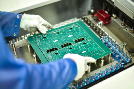
PCB Assembly Production Process
Contact us for a quote
1. Material examination and preparation PCBAMAKE Components Procurement team works concurrently with our PCB Fabrication team to ensure that all assembly materials are received and ready for use as soon as the bare PCBs are ready for assembly. As components are received at PCBAMAKE production facility, our Incoming Quality Control (IQC) team conducts a thorough inspection of any particlular material or components before warehousing.
Inspections include sample operational testing as well as date code verification and entry into a software material management system. Our sophisticated software management system ensures that rules of first-in-first-out are strictly followed, and that parts used in PCB Assembly are always in good working order.
2. Stencil preparation We use a stencil in PCB SMT assembly so that we can perform solder paste printing at a fixed position. Therefore, we need to prepare the stencil as per our placements of solder pads.
3. SMT Solder paste printing Solder paste is basically a mixture of tin and flux. Used to connect pads and electronic components on the PCB. The first step in the actual PCB assembly process is to apply solder paste to the bare PCB. A stainless steel stencil created during PCB fabrication is mounted on the bare board, leaving only the pads for assembling surface mount components. The stencil is held in place by mechanical fixtures, and the applicator moves across the board surface to finely distribute the solder paste over those uncovered spaces.
Pcbamake quality control team then performs a thorough inspection to ensure that the solder has only been applied to the necessary areas, and that all pads are covered with a sufficient amount of paste. For double-sided SMT boards, this process will need to be performed individually for each side, as indicated in the above flowchart. Pcbamake solder of choice is DELTA the best solder paste in China and worldwide , which is a Lead-Free alloy containing 96.5% tin, 3% silver, and 0.5% copper, and is compliant with the RoHS, REACH, and JEIDA directives. We use the paste version of this material for reflow soldering, and solid versions for manual and wave soldering.
4. SMT placement Once solder paste is applied to the bare PCBs, they are moved to Pcbamake’s automated Pick & Place machines for the actual mounting of components on their associated pads. Part placement is 100% machine automated for maximum accuracy and efficiency, and uses the project’s pickplace file for component coordinates and rotation data. The boards are again inspected after components have been mounted to ensure all placements are accurate before the soldering process begins.
5. Reflow soldering After placing the components on the PCB, we place them in a reflow soldering oven. The heating is done in various stages. And each stage refers to a specific heating zone. So, these stages are as follows:
Pre-heat Zone
Soaking Zone
Reflow Zone
Cooling Zone
If the PCB is double-sided then we might have to repeat all of these processes for the other side as well.
6. AOI Automatic Optical Inspection Pcbamake new AOI automatic optical inspection machines are running now for both prototype PCB and mass production. Pcbamake 100% AOI tested PCBAs:Automated optical inspection (AOI) is an automated visual inspection of printed circuit board (PCB) (or LCD, transistor) manufacture where a camera autonomously scans the device under test for both catastrophic failure (e.g. missing component) and quality defects.
7. X-Ray Inspection After a reflow cycle, any boards including BGA, QFN, or other lead-less package types are sent for X-Ray Inspection.
X-Rays penetrate the silicon of an IC package and reflect from the metal connections underneath, forming an image of the solder joints themselves that can be analyzed by advanced image processing software similar to Automated Optical Inspection (AOI). Higher-density features in the captured area create a darker resulting image, allowing for quantitative analysis to determine quality of the solder joints and compare against industry standards.
Not only does X-Ray inspection detect issues in PCB assembly, but the analysis of an X-Ray image can help to determine the root cause of a given defect, such as insufficient solder paste, skewed part placement, or improper reflow profile.
8.Wave Soldering Wave soldering is a method of PCB Assembly that involves sending boards on a conveyor through a “wave” of molten solder. The solder bonds together exposed component pads and leads while wicking off of the bodies of components and the solder masked bulk of the board.
The growing popularity of surface mount parts and HDI PCB layouts make reflow soldering the method of choice for a majority of projects, and manual soldering can be used to take care of the typically few components not suitable for reflow.
For traditional boards that require a high percentage of through-hole assembly, as well as boards that contain large connectors with very high pin counts, wave soldering generally remains the most efficient method of PCB assembly.
9. Cleaning and Inspecting Then we clean the PCBs and look for any inherent defects. If no defects are found then the PCB is good to go. Otherwise, we will have to perform repair or rework. Therefore, we use various equipment for performing the inspection. These include FAI, AOI,X-ray machine, etc.
10.Packing and delivery We can provide any packaging services for customer needs, include ESD bags or cartons packaging,reusable carton packaging, customized ESD plastic containers,ESD suitable product-specific trays,etc.,and finally send the product to your hands in the fastest and safest way. We cooperate with major logistics companies, of which DHL can achieve 60%-70% off to give your best service at the least price.