PCB Design & Layout Service
PCBAMake has an excellent PCB design team that can quickly and efficiently provide complete engineering and pcb design services, from concept to production.
 
With over 20 years of experience and knowledge in different industries, we use the industry's top pcb design tools and have the ability to think outside the box and create innovative designs and reliable manufacturing solutions.
 
PCBAMake design team are sophisticated with printed circuit board design and layout services for 20+ years in terms of medical devices, musical instruments, RF converter, smart consumer products, system controllers for solar power, temperature & humidity monitor, IOT units etc
 
Up to now, PCBAMake pcb layout team are capable of dealing with flex-rigid PCB layout with 20 layers at most. Apart from above PCB design, PCBAMake layout team also provides professional layout service on high-speed PCB and high-frequency PCB design, analog, digital and analog-digital signal arrangement etc.
 
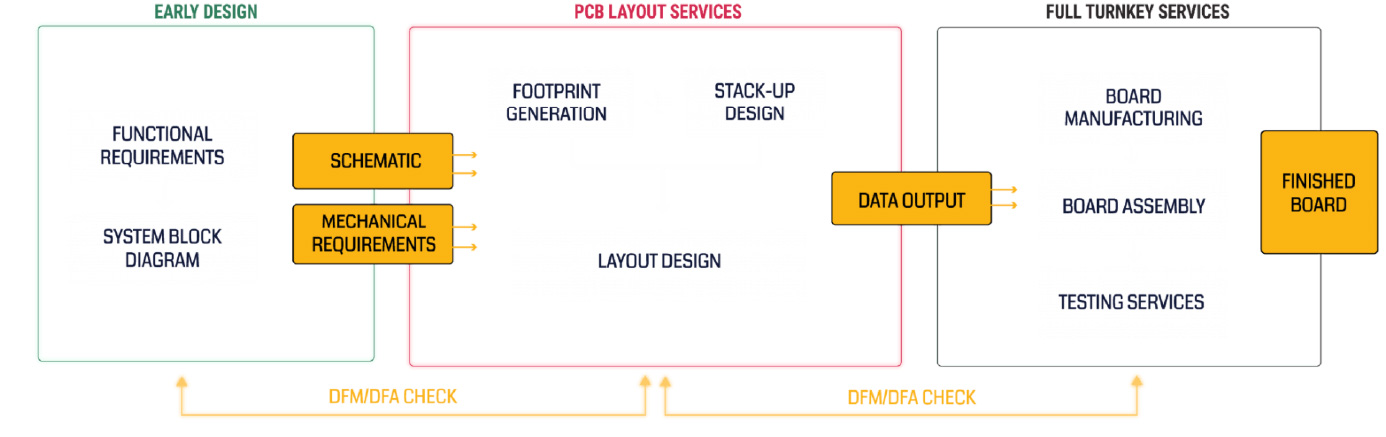
PCBAMake  can transfer your excellent concept into product quickly as long as you send us requirements (such as functions, shape, drawings etc.). We can complete PCB design and make PCB prototype accordingly. Design job includes schematics, layout, components selection, circuit simulation and software etc. In order to shorten your timeline, we comply with strict standards to handle PCB design phases, such as from requirement draft, alpha & beta review to volume production. In this case, your PCB design tasks go smoothly under our project management team.
 
PCB design needs to provide information:
1. Schematic diagram: a complete electronic document format that can generate the correct netlist;
2. Mechanical size: Provide the specific position and direction identification of the positioning device, as well as the identification of the specific height limit position area;
3. Device packaging: provide device packaging library or electronic material specification;
4. Wiring Guide: Description of specific requirements for special signals, as well as design requirements for impedance, stacking, etc.
PCB Design, PCB Layout
 
 
Our PCB Design Service 
We help our customers design and manufacture innovative world-class goods for the high-tech industry, propelling their businesses into new orbits. We also provide ongoing after-sales support through our technical consultants. Designing and manufacturing cutting-edge electronic and automation systems for businesses, industries, and individuals worldwide is our niche.
 
We’ve created a tight-knit team of engineers and managers who specialize in the following prospective markets: E-CAD, Firmware Development, Embedded systems development, power electronics system, IoT during the last five years. We are prepared to take on specific development and production tasks to finish your project on a turnkey basis.
Board Design
System & Board Level Architecture Specification
Engineering Design Specification
Component Selection
Component Obsolescence & Planning
Symbol Creation
Schematic Drawing/Capture
Timing Analysis
Netlist Generation
BOM Generation
Tools: (OrCAD, Concept HDL Altium, PADs, Expedition)
 
PCB Layout
Footprint Creation
Placement
Routing
Power DC Drop Simulation
Power Integrity and Signal Integrity Simulation
Gerber Generation
Tools: (Allegro, Altium, PADs, Expedition)
 
 
Capabilities Of Our Pcb Design Services
  • Multilayers, flexible and complex engineering like HDI, impedance control, blind & buried vias.
  • EMI/EMC protection
  • High-speed signal design
  • Sensitive analog circuits
  • Design for manufacturability and testability
  • Compatible with popular design software including Altium Designer, Cadence OrCAD/Allegro, Legacy PCAD, Eagle (Altium Conversion)
  • Scientific design workflows including schematic capture, PCB stack-up design, reverse engineering, cost optimization, signal integrity
The highest design layer 56 floors
Maximum design PIN number 110000+
Maximum number of connections 78000+
Minimum line width 2.4mil
Minimum line spacing 2.4mil
Minimum via 6mil (4mil laser hole)
Maximum BGA PIN Pitch 0.4mm
Maximum BGA PINs 3600+
highest speed signal 10G CML differential signal
 
Our Advantages
Board Design
System & Board Level Architecture Specification
Engineering Design Specification
Component Selection
Component Obsolescence & Planning
Symbol Creation
Schematic Drawing/Capture
Timing Analysis
Netlist Generation
BOM Generation
Tools: (OrCAD, Concept HDL Altium, PADs, Expedition
Focus on complex PCB design
Focus on complex PCB design            
Everything starts from reality
Everything starts from the customer's point of view
And fully communicate with customers for layout
Develop constraint rules, perform routing and optimize routing
Post-processing the PCB for beautification
Track PCB production to solve problems encountered in the production process
Assist customers with testing
PCB Design capabilities
Maximum PCB design layers: 32 layers
Maximum number of PINs: 110000+
Maximum number of connections: 78000+
Minimum line width: 2.4mil
Minimum line spacing: 2.4mil
Minimum via: 6mil (4mil laser hole)
Maximum number of BGAs: 120+
Minimum BGA PIN pitch: 0.3mm
Maximum number of BGA PINs: 8371
Highest speed signal: :112G-PAM4
PCB Layout
Footprint Creation
Placement
Routing
Power DC Drop Simulation
Power Integrity and Signal Integrity Simulation
Gerber Generation
Tools: (Allegro, Altium, PADs, Expedition)
 
 
Our Pcb Design Workflow


FAQ

Q

How long have you been making PCB&PCBA?

A

PCBAMake has been making PCBs for more than 26 years.We built our assembly plant and begin assembly business in 1996.

Q

How do I get a quick quote for PCB or PCB assembly?

A

Please send your files and requirements to Orders@pcbamake.com.Quote will be sent back as soon as we get through an evaluation.

Q

Do you cater SMT prototype boards?

A

Yes, we are fully equipped to handle your any kind of custom SMT prototype board requirements.MOQ is 1PCS.

Q

What files and documents do you request for my PCBA orders?

A

Gerber Files/Bill of Materials, complete information in excel format/Centroid Data/Other requirements or assembly instructions if applicable.

WHAT CAN I DO FOR YOU ?

Submit