Why should PCB testing be required?
For any designer or builder to be ultimately successful, a PCB test method must be implemented. By testing your pcb board, you can minimize major problems, find smaller bugs, save time and reduce overall costs.
PCB testing is primarily used to mitigate issues throughout the manufacturing process as well as the final production process. These types of tests can also be used on prototypes or small-scale assemblies, which can help identify potential problems that may exist in the final product.
An engineer can only control so much with regards to component tolerances, part-to-part variation, noise immunity/emission and general specifications or call-outs in a drawing for PCB fabrication or PCB assembly.
What to test on PCBs
A PCB consists of several different parts and components. Each of these has an impact on the overall performance of the circuit and the electronics assembly as a whole. Ideally, it is important to test everything. This includes, but not limited to verifying the;
Electrical conductivity
Mechanical strength
Soldering quality
Cleanliness
Tests for the target environment
Lamination — peel strength
Quality of hole wall
Component placement, alignment, polarity, orientation, etc.
PCB Inspection & Testing Services Of PCBAMake
Manual / Visual Inspection
Visual inspection is a manual approach of testing that requires experienced inspectors who can determine what is acceptable and what is not. 
This step can be used for printed circuit board inspection during assembly. The equipment used for visual inspection is selected according to the inspection target. Through this inspection, printed circuit boards and their components and assemblies are also thoroughly inspected. This is the most cost-effective inspection.
Automatic Optical Inspection (AOI)
AOI uses a vision system to capture an image of the circuit. By comparing this image to an expected image and to a set of design rules, image errors are detected. AOI machines detect flaws by a combination of design rule checks and comparison to design data. 
PCBAMake AOI automatic optical inspection machines are running for both prototype PCB and mass production.PCBAMake 100% AOI tested PCBAs:Automated optical inspection (AOI) is an automated visual inspection of printed circuit board (PCB) (or LCD, transistor) manufacture where a camera autonomously scans the device under test for both catastrophic failure (e.g. missing component) and quality defects.
 
Area defects Flipped component Severely Damaged Components
Billboarding Height Defects Tombstoning
Component offset Insufficient Paste around I Leads Volume Defects
Component polarity Insufficient Solder Joints Wrong Part
Component presence or absence Lifted Leads Solder Bridging
Component Skew No Population tests Presence of Foreign Material on the board
Excessive Solder Joints Paste Registration  
AOI can be used in the following locations in the SMT lines: post paste, pre-reflow, post-reflow, or wave areas.
Microsection Inspection
Inspection method that examines the integrity of through-holes, laminate system, solder joint interfaces and other structures in and on the PCB.
 
Samples are extracted from the board and are then evaluated under high magnification.
 
Microsection analysis is a destructive procedure but can reveal critical defects of designs that are close to or exceed typical manufacturing specifications/tolerances - a test that is generally worthwhile for mass-production volumes of complicated boards. It is a required test for military PCB and Class 3 PCB requirements.
Electrical Test
Electrical testing is the most common methodology used to determine if a board is good or bad. To electrically test a board requires that the board come into physical contact with a measurement system. There are two test types performed: continuity and isolation.
 
Continuity testing checks for the continuous path or appropriate interconnect of pads, traces and through holes.
For isolation testing, we are trying to determine if networks or traces are separated or isolated from each other.
The type of test equipment appropriate to an operation varies with the type of boards produced, level of testing required and a variety of other influences.
 
Most common test systems are Flying Probe testers. Each board requires the flying probe system to have unique programming (corresponding to the coordinates and test specs of each test point). As a result, this is a premium test but once configured and programmed, the testing process goes very quickly per board and, depending on annual volumes, is generally cost-effective in the long run.
 
Also, fixtured testers, with a dedicated test system and universal grid system, are used for testing medium to high-volume PCB production runs. A custom test fixture containing cabling/interfacing and systems that monitor specific signals could be well tailored to the design and test against high reliability and performance.
In-Circuit Test (ICT)
In-circuit testing is a popular PCB testing method that many PCB manufacturers prefer to employ, and it can find 98% of faults. This testing method uses special PCB testing steps and equipment, including:
 
In-circuit tester: The tester system contains a matrix of hundreds or thousands of drivers and sensors, which perform the measurements for the test.
 
Fixture: A fixture connects to the in-circuit tester and is the part that interacts directly with the board being tested. This fixture looks like a bed of nails and is designed specifically for the board in question. Each “nail,” or sensor point, connects to relevant points on the test board, feeding information back to the tester. Fixtures are generally the most expensive part of this system.
 
Software: Software for the tester instructs the system on what tests to perform for each type of board being tested and dictates the parameters for a pass or fail.
 
Using the ICT method, a manufacturer can test individual components and measure their performance, regardless of the other components attached to them. Generally, this type of testing is best for 3analog circuits since it’s best at measuring resistance, capacitance and other analog measures. Additionally, the cost of the equipment means that this testing method is best suited for the final testing of stable, high-volume products, not for low-volume productions or early testing stages where the design may change multiple times.
Fixtureless In-Circuit Test (FICT)/Flying Probe Test
The fixtureless in-circuit test (FICT), also known as the flying probe test, is a type of ICT that operates without the custom fixtures, reducing the overall cost of the test. First introduced in 1986, FICT uses a simple fixture to hold the board while test pins move around and test relevant points on it using a software-controlled program. Since its introduction, FICT has gained widespread use throughout the electronics manufacturing industry for its versatility.
 
FICT testing is used for the same things as traditional ICT, but because of the way it goes about testing, it offers different advantages and disadvantages. While FICT is able to adapt to new boards quickly, easily and cost-effectively, with a simple programming change, it tends to be slower than the traditional ICT. This quality makes it an ideal testing method for small-production tests and prototype testing but less effective for large-scale production.
Functional Circuit Test
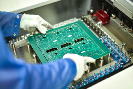
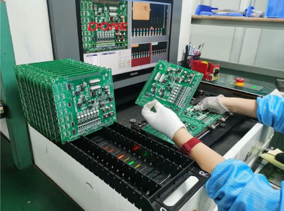
A functional circuit test is exactly what it sounds like — it tests the function of the circuit. This type of testing always comes at the end of the manufacturing plan, using a functional tester to check whether a finished PCB performs to specifications.
 
Some answers to common questions about functional circuit tests and how they work can be found below:
 
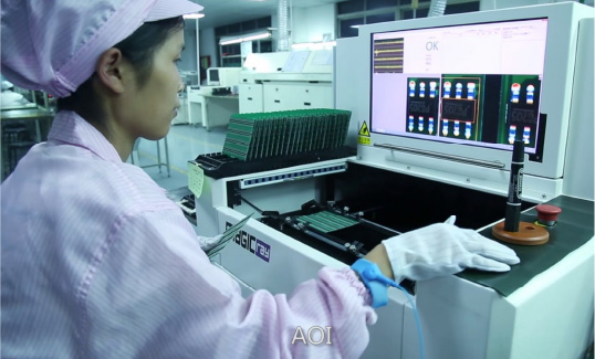
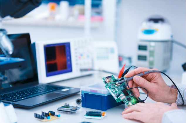
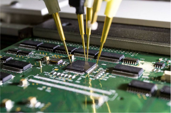
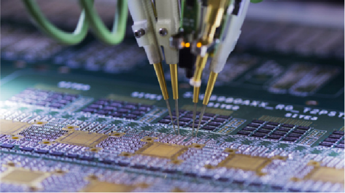
How do functional testers work? Functional testers come in several types but generally share the same function — they simulate the final environment in which the PCB is supposed to function. Functional testers usually do so by interfacing with the PCB via its test-probe points or edge connectors and testing to certify that the PCB functions according to design specifications.
 
Are functional circuits the same as ICTs? In some ways, functional circuit tests are similar to ICTs in that they use connectors to attach to the board. In the case of functional circuit testers, they use pogo pin devices to connect to the PCB and generally need fewer pins than an ICT fixture. The test equipment then runs programs to test the PCB, ensuring that the equipment functions exactly as intended.
 
When do functional circuit tests occur? As previously stated, functional circuit tests are the last type of test to complete in a PCB manufacturing plan, ensuring that the product going out functions according to specifications.
What does a functional circuit test evaluate? Generally, functional circuit tests just look at the product’s functionality as a whole and grade it on a pass or fail basis. As a result, it’s not an ideal testing method for early prototypes since it doesn’t identify details about what’s wrong with the product.
PROTECT YOUR PCB WITH BETTER DESIGNS
To better protect your PCB and have it pass an inspection and test, you may want to consider utilizing some of the top design techniques available today. Design for Manufacturing (DFM), Design for Assembly (DFA), Design for Test (DFT) and Design for Supply Chain (DFSC) are all some of the best design techniques used to ensure a PCB is manufactured correctly.
Design for Manufacturing
DFM is the process of arranging a PCB topology with the manufacturing process in mind. With this design mentality, the PCB layout topology is intended to mitigate problems that typically occur during the fabrication and assembly processes, including:
 
Slivers and islands: Pieces of free-floating copper on a PCB layer can cause issues in a PCB design, which tends to happen when a design includes several areas with small islands of copper between traces. These pieces can break away and cause interference on other parts of the board and islands, trace impedance, trace inaccuracies, impedance and other issues.
 
Solder bridges: When traces and pins are placed too close together and a solder mask isn’t used in a design, solder can create bridges between pins, causing shorts and corrosion along with other issues.
 
Copper to edge: Sometimes, the copper on a PCB is too close to the edge of the board, causing shorts to occur during the etching process when an electrical current is applied. DFM tests should be implemented early in a project timeline to reduce overall costs and development time. There are plenty of software programs available that identify issues like those listed above.
Design for Assembly
For any PCB assembly, it’s essential to attach components securely to the circuit board. Unfortunately, doing so can be difficult when the design is hard to assemble, which is why DFA is essential. With DFA, the goal is to determine how to design the PCB so that the assembler can complete their job quickly and effectively.
 
The DFA process includes the following steps:
Minimize material inputs.
Choose easily available components.
Give components an adequate amount of space between each other.
Apply general standards of PCB design.
Make markings for components accurate and clear.
 
Like DFM, DFA tests should be implemented early on in a project design process to minimize production costs and product development time. PCB testing software programs are available to help ensure PCB designs meet DFA standards.
Design for Test
DFT is a type of design that helps make testing more thorough and less costly. Essentially, PCBs designed with DFT in mind are designed to make it easy to detect and locate failures. This way, it’s easier to run tests quickly and accurately, reducing the amount of time needed for testing. For this to work, designers have to know exactly what type of testing methods they’ll be using at each stage of production and design the PCB to work optimally with them.
 
DFT can require a great deal of additional design and engineering effort in the PCB design process, easily making up for the amount of time saved during testing. The amount of time spent, however, is easily made up for with an overall decrease in manufacturing costs. With faults easier to find, it’s less likely for PCBs with hidden faults to be sent out, reducing the cost of customer dissatisfaction and potential recalls.
Design for Supply Chain
One thing that many designers don’t consider is the life cycle of a product or component. Often, certain components become obsolete during the product life cycle of a PCB, and it becomes more difficult to source that component in a cost-effective way. It’s essential to consider component life cycles when designing new products with DFSC techniques.
 
Staying aware of life cycles includes talking to an experienced electronics contract manufacturer to determine stock availability and alternate sourcing for the components of a PCB early in the design process. In the long run, this DFSC strategy will help save money by ensuring a long lifespan for a PCB design.


FAQ

Q

How long have you been making PCB&PCBA?

A

PCBAMake has been making PCBs for more than 26 years.We built our assembly plant and begin assembly business in 1996.

Q

How do I get a quick quote for PCB or PCB assembly?

A

Please send your files and requirements to Orders@pcbamake.com.Quote will be sent back as soon as we get through an evaluation.

Q

Do you cater SMT prototype boards?

A

Yes, we are fully equipped to handle your any kind of custom SMT prototype board requirements.MOQ is 1PCS.

Q

What files and documents do you request for my PCBA orders?

A

Gerber Files/Bill of Materials, complete information in excel format/Centroid Data/Other requirements or assembly instructions if applicable.

WHAT CAN I DO FOR YOU ?

Submit