poe@pcbamake.com


HDI can make product design more miniaturized and meet higher electronic performance
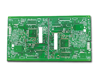
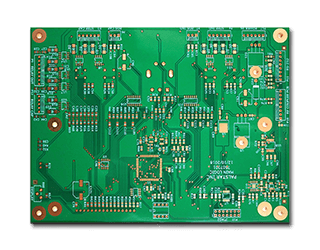
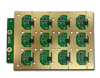
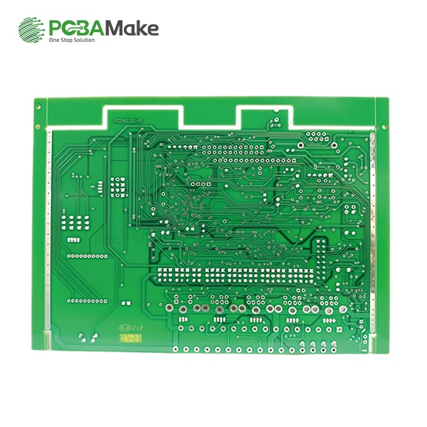
HDI PCB
Material: FR4 / FR4 TG180 / FR4 TG170
Finish treatment: Immersion Gold
Copper thickness: 1oz~ 2oz
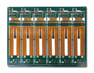
Resin plugging vias & Buried vias
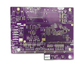
Impedance Controller Board
| Feature | Technical specification |
|---|---|
| Number of layers | 4 - 22 layers standard, 40 layers advanced |
| Technology highlights | Multilayer boards with a higher connection pad density than standard boards, with finer lines/spaces, smaller via holes and capture pads allowing microvias to only penetrate select layers and also be placed in surface pads. |
| HDI builds | 1+N+1, 2+N+2, 3+N+3,4+N+4, any layer in R&D |
| Materials | FR4 standard, FR4 high performance, Halogen free FR4, Rogers |
| Copper weights (finished) | 18μm - 70μm |
| Minimum track and gap | 0.075mm / 0.075mm |
| PCB thickness | 0.40mm - 3.20mm |
| Maximum dimensions | 610mm x 450mm; dependent upon laser drilling machine |
| Surface finishes available | OSP, ENIG, Immersion tin, Immersion silver, Gold fingers |
| Minimum mechanical drill | 0.15mm |
| Minimum laser drill | 0.10mm standard, 0.075mm advanced |
High Density Interconnect PCB, is a circuit board with relatively high line distribution density using micro-blind and buried via technology.
With the development of high-density, high-precision electronic products, the requirements for circuit boards are also the same. The most effective way to increase PCB density is to reduce the number of vias and precisely set blind and buried vias to meet this requirement, resulting in HDI boards.
The electrical interconnection between the board layers of HDI is realized through conductive through holes, buried holes and blind holes. Its structure is different from ordinary multi-layer circuit boards. A large number of micro-buried blind holes are used in HDI boards. HDI uses laser direct drilling, while standard PCBs are usually mechanically drilled, so the number of layers and aspect ratios tend to be reduced.
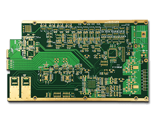
HDI can not only enable more miniaturization of end product designs, but also meet higher standards of electronic performance and efficiency at the same time.
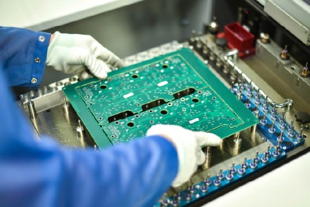
At present, the core pain point and difficulty of HDI manufacturing is the buried hole plug hole. If the HDI buried hole plugging is not done well, there will be major quality problems, including uneven board edges, uneven dielectric thickness, and potholes on the pads. POE is very professional in this area, we have many years of experience to meet different needs, specially customize HDI PCB of different difficulty for you.

Delivery Services

Verified by

Link Us on