• hdi1
  • hdi1
  • hdi1
  • hdi1
  • hdi1
  • hdi1
  • hdi1
  • hdi1
  • hdi1
  • hdi1
  • hdi1
  • hdi1

Multilayer PCBs

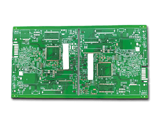
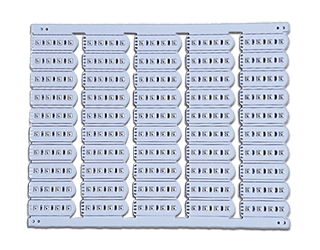
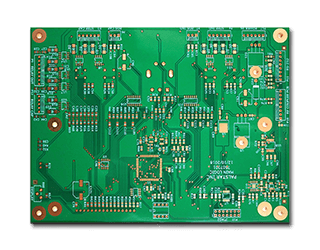
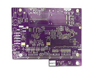
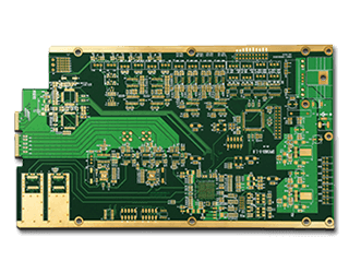
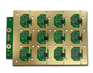
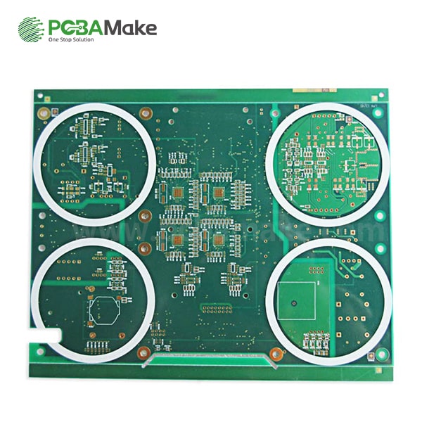
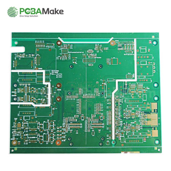
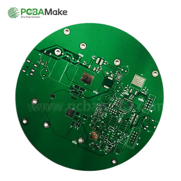
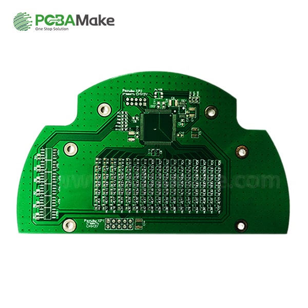
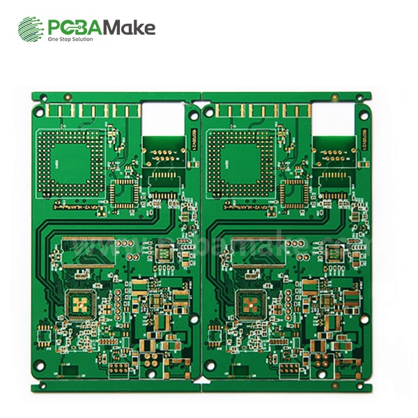
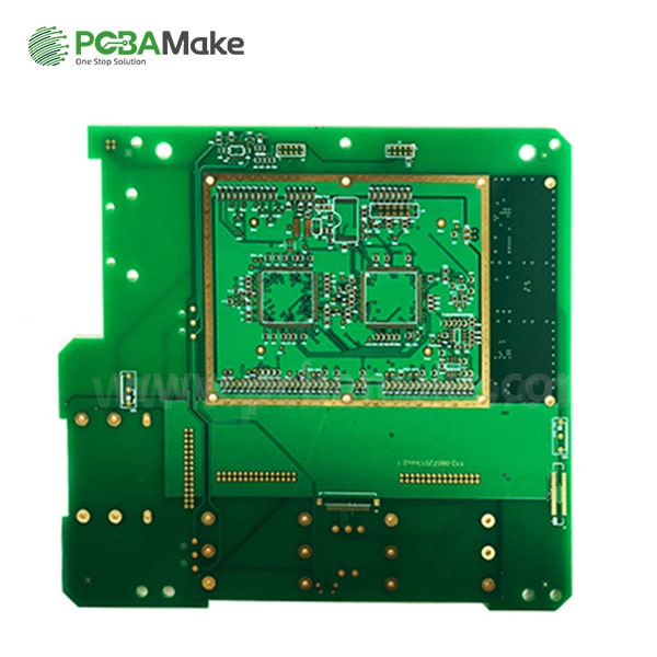
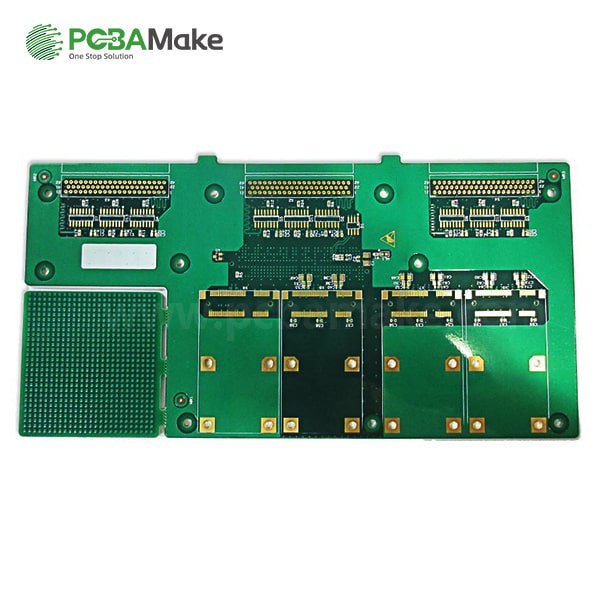
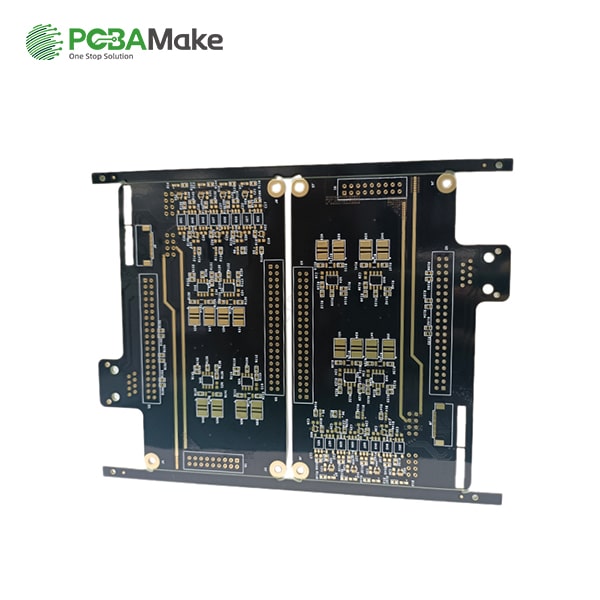
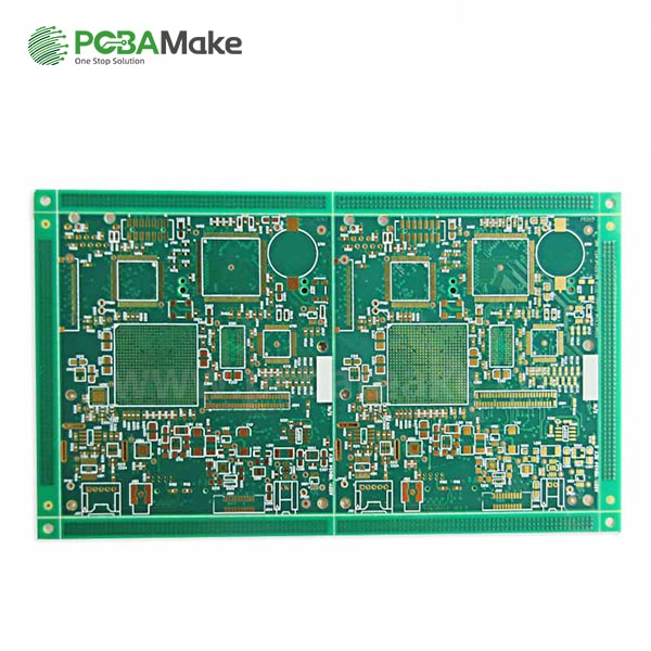
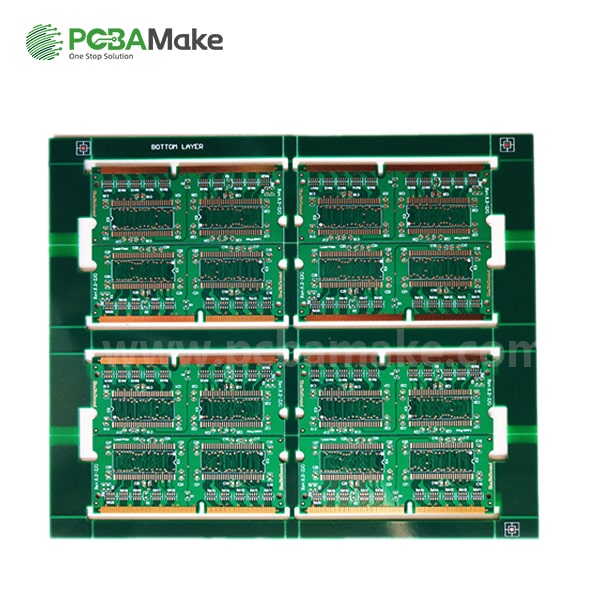
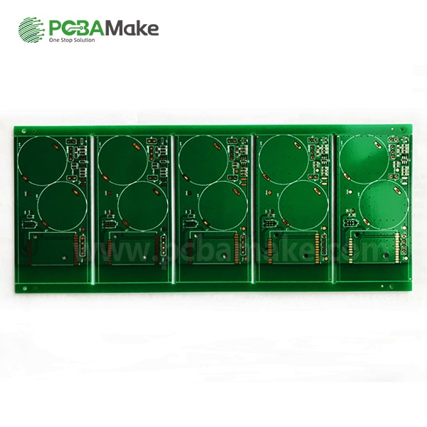
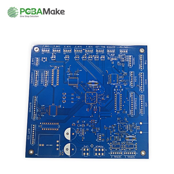
Multi layer PCB boards are suitable for complex devices with a large number of components and circuits in complex design.

Material: FR4,Polyimide,Aluminum,Teflon and others
Finish treatment: Immersion Gold
Copper thickness: 0.5oz~ 1oz
Surface Treatment: Immersion Gold/OSP/HASL
Solder Mask Color: Green/White/Blue/Red/purple/black

REQUEST A QUOTE
Multilayer PCBs – Technical specification
Feature Technical specification
Number of layers 1 - 40 layers
Technology highlights Multilayer boards with a higher connection pad density than standard boards, with finer lines/spaces, smaller via holes and capture pads allowing microvias to only penetrate select layers and also be placed in surface pads.
Silk Screen Color White/Black
Materials FR4 standard, FR4 high performance, Halogen free FR4, Rogers
Copper weights (finished) 18μm - 70μm
Minimum track and gap 0.075mm / 0.075mm
PCB thickness 0.40mm - 3.20mm
Maximum dimensions 610mm x 450mm; dependent upon laser drilling machine
Surface finishes available OSP, ENIG, Immersion tin, Immersion silver, Gold fingers
Minimum mechanical drill 0.15mm
Minimum laser drill 0.10mm standard, 0.075mm advanced
Multilayer PCB
With the continuous innovation of electronic technology and the continuous improvement of the requirements for electronic equipment in some industries such as computers, medical treatment, and aviation, printed circuit boards are developing in the direction of smaller volume, lighter weight, and increased density. Single and double-sided printed boards can no longer meet the demand, so it is necessary to consider using more layers and higher assembly density multilayer circuit boards.
What is a multilayer circuit board?
In daily life, multilayer PCB circuit boards are currently the most widely used circuit board type. Multilayer PCB are circuit boards composed of two or more conductive layers (copper layers) superimposed on each other. The most common is four Six-layer board, such as the familiar computers in our daily life. Single-layer and double-layer boards are easy to distinguish and can be distinguished with the naked eye. Hold the board and look at the light. Except for the wiring on both sides, the rest of the place is transparent . But for multilayer PCB boards with four-layer boards and six-layer boards, if there is no corresponding mark on the board, it is not so easy to distinguish. Generally, the requirements for the structure design and process production of multilayer electric boards are very high, and the higher the number of layers, the more difficult it is, and it is suitable for use in more complex circuits.

Application advantages of multilayer PCB circuit boards:
1. High assembly density, small size and light weight, meeting the needs of light and miniaturization of electronic equipment;
2. Due to the high assembly density, the wiring between each component (including components) is reduced, the installation is simple, and the reliability is high;
3. Due to the repeatability and consistency of the graphics, the errors in wiring and assembly are reduced, and the maintenance, debugging and inspection time of the equipment is saved;
4. Flexible design, larger wiring space;
5. It can form a circuit with a certain impedance and can form a high-speed transmission circuit;
6. Circuit, magnetic circuit shielding layer can be set, and metal core heat dissipation layer can be set to meet the needs of special functions such as shielding and heat dissipation.
Multilayer PCB Production Process
PCB Product Listing
Multilayer PCB
Rigid Fex PCB 
Aluminum PCB
HDI PCB
Flexible PCB 
Rigid PCB
High tg PCB
High Frequency PCB