How is PCB board copying achieved?
Specific steps and methods of PCB board copying
PCB board copying is a complex and delicate process involving multiple steps.
Specific steps and methods of PCB board copying
1. Preliminary preparation
Component record:After getting a PCB, first record the model, parameters and position of all components on paper, paying special attention to the direction of diodes, triodes and IC notches.
Use a digital camera to take photos of the component positions to ensure that the records are complete and accurate.

2. Component disassembly and bill of materials preparationRemove components:Remove all components, clean the tin in the PAD holes, and clean the PCB with alcohol.
Bill of materials BOM preparation:
Make the removed components into a bill of materials (BOM) and arrange material procurement to ensure accurate restoration in the subsequent assembly process.
3. PCB image scanning
Scanning PCB:
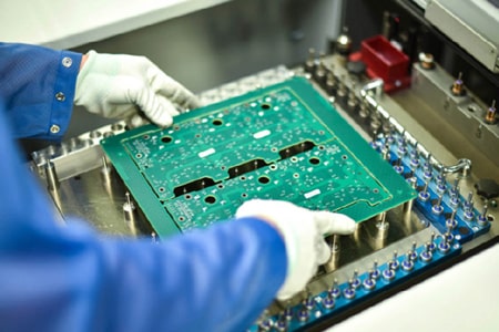
Put the cleaned PCB into the scanner and adjust the scanning pixels to obtain a clear image. Use color to scan the top and bottom layers separately and save them as high-quality image files.
Use water sandpaper to lightly polish the top and bottom copper films again, scan and generate new images, and ensure that the copper film part and the non-copper film part have a clear contrast.
4. Image processing and file conversion
Image processing:
Adjust the contrast and brightness of the image in PHOTOSHOP, convert it to black and white, and ensure clear lines. Save it as a black and white BMP format file (such as TOP.BMP and BOT.BMP).
File conversion:
Use the copy board software to convert the BMP format file to the PROTEL format file. Import the two layers of images in PROTEL, check the alignment of the PAD and VIA positions, and ensure accuracy.
5. PCB drawing
Drawing the circuit diagram:
Convert the BMP of the TOP layer to the TOP.PCB file, draw the circuit on the TOP layer and place the components according to the recorded drawing. After drawing, delete the SILK layer and repeat this step to complete the drawing of all layers.
Synthesize PCB diagram:
Input TOP.PCB and BOT.PCB in PROTEL to synthesize a complete PCB diagram. Use a laser printer to print the transparent films of TOP LAYER and BOTTOM LAYER respectively, and compare and check the accuracy of the graphics.
6. PCB production and component welding
PCB production:
Send the generated PCB file to the plate-making factory for plate-making to obtain a new PCB board.
Component welding:
Weld the purchased components to the newly made PCB board to ensure the welding quality and accurate position.
7. Circuit board testing and debugging
Testing and debugging:
Perform electrical performance testing and debugging of the circuit board to ensure that the electronic performance of the copied PCB is consistent with the original board.
Double-sided and multi-layer board copying method
Double-sided board copying method
Scan the upper and lower surfaces of the circuit board and save two BMP images.
Use Quickpcb2005 software to draw the circuit layer by layer and place components to generate a B2P file.
Open the previously saved B2P file, close the top-level circuit and silk screen, leaving only the multi-layer vias, then draw the bottom-level circuit, save and export it as a PCB file.
Multilayer board copying method
Multilayer board copying requires repeated copying of multiple double-sided boards, grinding out the inner layer image layer by layer through layering technology, drawing and converting, and finally synthesizing it into a multilayer PCB file.
How is PCB board copying achieved? Knowledge points on the specific steps and methods of PCB board copying. If you want to know more, you can pay attention to PCBAMake. If you need to know more about PCB proofing, SMT patch, and PCBA processing related technical knowledge, please leave a message to get it!

