Requirements and considerations for PCB silk screen design
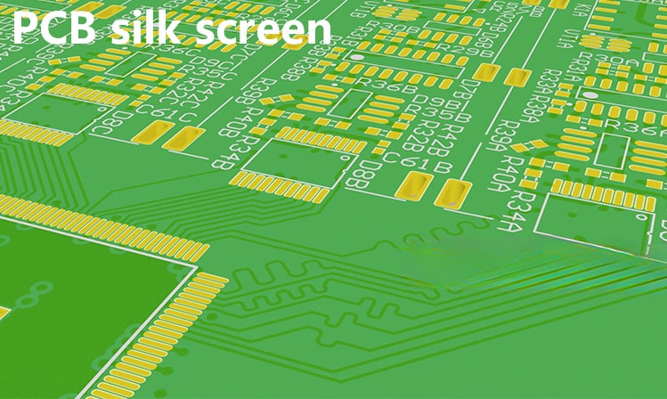
The silk screen layer of the PCB is used to identify components, test points, and other important information to help engineers better understand the layout of the circuit board during manufacturing, assembly, and maintenance. The following are some requirements and considerations for designing silk screen.
Requirements and considerations for PCB silk screen design:
Clear and readable text: Ensure that the text on the silk screen is clear and readable, and choose the appropriate font and text size so that it can be easily identified during manufacturing and use.
Component identification: Indicate the name, model, and value of the component in the silk screen to facilitate maintenance and repair. Ensure that the position of the logo does not block the component or affect welding.

Pin marking: Indicate the pin number around the pin of the component to facilitate welding and debugging. Use clear pin markings, such as numbers or letters.
Direction indication: Indicate the direction of the PCB, usually with an arrow or other indicative symbol. This is essential to ensure the correct direction during assembly and use.
Layer marking: Indicate the corresponding layer information on the top and bottom layers of the PCB so that it can be accurately identified during manufacturing and maintenance.
Specify graphics and lines: Keep graphics and lines clear and avoid overly complex silkscreen designs that affect production quality.
Appropriate spacing: The spacing between silkscreen and components, pads, etc. should be sufficient to avoid affecting welding and assembly processes.
Material selection: Choose corrosion-resistant and wear-resistant silkscreen materials to ensure that the silkscreen remains clearly visible during the service life of the PCB.
Contrast: Choose a silkscreen color with a large contrast with the PCB color to ensure that it is still easy to identify under different lighting conditions.
Avoid occlusion: Avoid silkscreen occluding key components or signal paths to ensure that the underlying circuit can be clearly seen when necessary.
When designing PCB silkscreen, it is best to refer to the specifications and recommendations of the PCB manufacturer to ensure that the requirements of its equipment and processes are met. Using professional PCB design tools makes it easier to add and manage silkscreen information.
High-quality silkscreen design can improve the manufacturability and maintainability of PCBs. Designers need to pay attention to the rationality and aesthetics of the layout while ensuring the integrity of the information. By following the above requirements and precautions, the design quality and use efficiency of PCBs can be effectively improved.
If you want to know more, you can follow PCBAMake. If you need to know more about PCB proofing, SMT patch, and PCBA processing related technical knowledge, please leave a message to get it!

