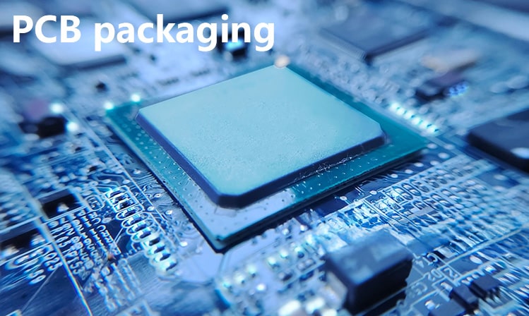
PCB packaging
In the field of electronic design and manufacturing, PCB is an indispensable core component, and PCB packaging is the bridge between electronic components and PCB. Efficient and accurate packaging design can directly affect the performance of the circuit and the reliability of the product
1. What is PCB packaging
PCB packaging is to express the various parameters of actual electronic components (such as chips, resistors, capacitors, etc.) (such as size, length and width, direct plug-in or patch, pad size, pin length and width, pin spacing, etc.) in a graphical way, so as to facilitate calling when drawing PCB diagrams. These graphical packaging information includes the shape and symbol of the component, the number of pads, position, reference pins, polarity, etc., which is the basis of PCB design and manufacturing.

2. Types of PCB packaging
PCB packaging can be divided into many types according to installation method, pin shape, packaging material, etc. The following are some common PCB packaging types:
BGA packaging (Ball Grid Array):
Spherical contact display, one of the surface mount packaging.
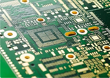
Ball bumps are made in an array on the back of the printed substrate to replace the pins, and the LSI chip is assembled on the front of the printed substrate, and then sealed with molded resin or potting method.
It has a large number of pins and good heat dissipation performance, which is suitable for high-density circuit boards.
DIP package (Double In-line Package):
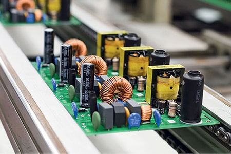
Dual in-line package, one of the plug-in packages. It usually needs to be soldered through the through-holes on the PCB. It is suitable for traditional through-hole plug-in technology (THT). The pins are led out from both sides of the package, and the packaging materials are plastic and ceramic. It is easy to plug and unplug, but it is not suitable for PCB boards with high-density layout.
Application: Common in early analog circuits, power devices and some microcontrollers.
Advantages: Easy to manually solder and debug.
Disadvantages: It occupies a large PCB area and is not suitable for high-density circuit design.
SOP package (Small Outline Package):
Small outline package integrated circuit, a very common component form. The pins extend from both sides and are soldered on the PCB surface. Later, SOJ (J-type pin small outline package), TSOP (thin small outline package), VSOP (very small outline package), SSOP (shrink SOP), etc. were gradually derived.
Application: widely used in consumer electronic products, such as microprocessors, memory chips, operational amplifiers, etc.
Advantages: small size, light weight, suitable for automated production.
Disadvantages: high pin density, high welding requirements.
QFP package (Quad Flat No-lead Package):
Four-sided no-lead flat package integrated circuit, a pinless package. There is a small square in the center of the bottom for heat dissipation. The pins of the QFP package are distributed around the chip, which is suitable for chip design with a high number of pins. There are three types of substrates: ceramic, metal and plastic. Plastic QFP is a commonly used multi-pin LSI package.
Application: Commonly used in high-performance chips such as MCU (microcontroller), DSP (digital signal processor), FPGA, etc.
Advantages: many pins, suitable for complex circuits.
Disadvantages: pins are easy to bend, and the welding process requirements are high.
PLCC package (Plastic Leaded Chip Carrier):
Plastic chip carrier with leads, one of the surface mount packages.
The pins are led out from the four sides of the package in a T-shape, and are plastic products.
J-shaped pins are not easy to deform and are easier to operate than QFP, but the appearance inspection after welding is more difficult.
COB package (Chips on Board):
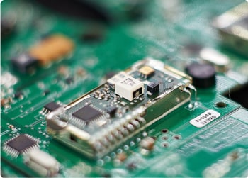
Chip mount package, the chip is directly attached to the PCB.
Usually used for small and highly integrated applications.
3. The role of PCB packaging
Protect electronic components: Through packaging, electronic components can be isolated from the external environment to prevent dust, moisture, chemicals, etc. from damaging electronic components.
Improve reliability: The package can fix electronic components to prevent them from mechanical damage during transportation, installation and use.
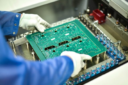
Easy to assemble and maintain: Through standardized packaging, it is easy to insert or weld on the PCB, which improves assembly efficiency. At the same time, the package also provides identification information for electronic components, which is convenient for subsequent maintenance and management.
4. Precautions for PCB packaging
Choose the appropriate package type: According to the characteristics of the electronic components and the requirements of the PCB board, choose the appropriate package type. For example, for high-density circuit boards, you can choose BGA packaging; for components that need to be frequently plugged and unplugged, you can choose DIP packaging.
Pay attention to package size and pin spacing: The package size and pin spacing need to match the pad size and spacing on the PCB board to ensure the reliability and stability of welding.
Consider packaging materials and processes: The selection of packaging materials and processes will also affect the performance and reliability of electronic components. For example, molded resin packaging has good mechanical strength and heat resistance; while potting methods can provide better moisture and dust resistance.
PCB packaging is an integral part of the electronic manufacturing process. By selecting the right package type, paying attention to package size and pin spacing, and considering factors such as packaging materials and processes, the reliability and stability of electronic components on PCB boards can be ensured.

