What is the impact of DFM on SMT patch processing?
The importance of DFM to SMT patch processingIn the field of electronic manufacturing, SMT (Surface Mount Technology) patch processing, as an efficient and precise electronic assembly method, provides strong support for the miniaturization and high performance of electronic products. However, the success of SMT patch processing depends largely on the DFM (Design for Manufacturing) considerations in the design stage. The full application of DFM can not only reduce production costs and improve production efficiency, but also directly affect the quality and reliability of the final product.

The core concept of DFM manufacturability design
DFM manufacturability design is a design concept, the core of which is to fully consider various factors in the subsequent manufacturing process during the product design stage. Improve production efficiency, reduce costs, and ensure product quality through optimized design. In SMT patch processing, the main goal of DFM is to optimize circuit board layout, reasonably select components, and optimize welding processes.
The importance of DFM to SMT patch processing
1. Improve production efficiency: DFM design can make the component layout of the circuit board more reasonable, reduce the moving distance and time during the mounting process, and thus improve the overall efficiency of the production line. Reasonable layout can also reduce errors and rework rates in the production process, further improving production efficiency.
2. Reduce costs: DFM design can foresee potential problems in the manufacturing process and optimize them in advance. This helps to avoid a large number of subsequent modifications and rework, saving manpower, material and time costs. In addition, selecting components and processes that meet DFM requirements can further reduce procurement and processing costs.
3. Ensure product quality: DFM design can fully consider the requirements of the welding process and ensure the stability and reliability of components during the welding process. Reasonable layout and component selection can reduce stress and deformation during welding and reduce the risk of welding defects. At the same time, DFM design can also help improve the testability and maintainability of the product, ensuring that the product can maintain high-quality performance throughout its life cycle.
Key considerations and strategies of DFM in practical applications
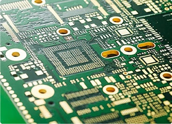
1. Circuit board layout optimization: The mounting accuracy and efficiency of the SMT placement machine need to be considered in the design stage, so that the component layout is reasonable, the spacing is moderate, and the orientation and pin arrangement are convenient for welding and inspection.
2. Component selection: Select components that meet DFM requirements, including factors such as package type, dimensional accuracy and pin spacing, to ensure easy mounting and welding, and meet product performance requirements.
3. Welding process optimization: Fully consider and optimize the welding process in the design stage, select appropriate welding methods and parameters, and formulate reasonable welding sequence and temperature curve to ensure a stable and reliable welding process.
Strategies to cope with challenges
DFM may face challenges such as team communication, design software functions and new technology applications in actual applications. To this end, we can strengthen communication and collaboration between teams, improve design software functions, pay attention to the development of new technologies and new processes, and introduce and apply them in a timely manner.
PCBAMake pcb assembly manufacturing plant provides free DFM inspections. If you need to learn more about PCB proofing, SMT patch, PCBA processing related technical knowledge, please leave a message to get it!


